Thursday, October 6, 2011

CouponDunia - Best way to grab best coupons

Want to do shopping with less expenditure and more savings??
CouponDunia provides you the best way to shop more and pay less by offering you discount coupons for more than 100+ sites.
Experience a new way for online shopping!!

So what are you waiting for???
Just visit


HAPPY SHOPPING!!!!


Monday, July 11, 2011

FET


The 'field-effect' transistor (FET) relies on an electric field to control the shape and hence the conductivity of a channel of one type of charge carrier in a semiconductor material. FETs are sometimes called unipolar transistors to contrast their single-carrier-type operation with the dual-carrier-type operation of bipolar (junction) transistors(BJT). The concept of the FET predates the BJT, though it was not physically implemented until after BJTs due to the limitations of semiconductor materials and the relative ease of manufacturing BJTs compared to FETs at the time.


History
The principle of field-effect transistors was first patented by Julius Edgar Lilienfeld in 1925 and by Oskar Heil in 1934, but practical semi-conducting devices (the JFET, junction gate field-effect transistor) were only developed much later after the transistor effect was observed and explained by the team of William Shockley at Bell Labs in 1947. The MOSFET (metal–oxide–semiconductor field-effect transistor), which largely superseded the JFET and had a more profound effect on electronic development, was first proposed by Dawon Kahng in 1960

Terminals


All FETs have a gatedrain, and source terminal that correspond roughly to the basecollector, and emitter of BJTs. Aside from the JFET, all FETs also have a fourth terminal called the bodybasebulk, or substrate. This fourth terminal serves to bias the transistor into operation; it is rare to make non-trivial use of the body terminal in circuit designs, but its presence is important when setting up the physical layout of an integrated circuit. The size of the gate, length L in the diagram, is the distance between source and drain. The width is the extension of the transistor, in the diagram perpendicular to the cross section. Typically the width is much larger than the length of the gate. A gate length of 1 µm limits the upper frequency to about 5 GHz, 0.2 µm to about 30 GHz.
The names of the terminals refer to their functions. The gate terminal may be thought of as controlling the opening and closing of a physical gate. This gate permits electrons to flow through or blocks their passage by creating or eliminating a channel between the source and drain. Electrons flow from the source terminal towards the drain terminal if influenced by an applied voltage. The body simply refers to the bulk of the semiconductor in which the gate, source and drain lie. Usually the body terminal is connected to the highest or lowest voltage within the circuit, depending on type. The body terminal and the source terminal are sometimes connected together since the source is also sometimes connected to the highest or lowest voltage within the circuit, however there are several uses of FETs which do not have such a configuration, such as transmission gates and cascode circuits.

Thursday, June 30, 2011

All types of Abbreviations

A
a. (in Etym.)     adoption of, adopted from
a (as a 1850)     ante, 'before', 'not later than'
a.     adjective
abbrev.     abbreviation (of)
abl.     ablative
absol.     absolute, -ly
Abstr.     (in titles) Abstract, -s
acc.     accusative
Acct.     (in titles) Account
A.D.     Anno Domini
ad. (in Etym.)     adaptation of
Add.     Addenda
adj.     adjective
Adv.     (in titles) Advance, -d, -s
adv.     adverb
advb.     adverbial, -ly
Advt.     advertisement
Aeronaut.     (as label) in Aeronautics; (in titles) Aeronautic, -al, -s
AF., AFr.     Anglo-French
Afr.     Africa, -n
Agric.     (as label) in Agriculture; (in titles) Agriculture, - al
Alb.     Albanian
Amer.     American
Amer. Ind.     American Indian
Anat.     (as label) in Anatomy; (in titles) Anatomy, - ical
Anc.     (in titles) Ancient
Anglo-Ind.     Anglo-Indian
Anglo-Ir.     Anglo-Irish
Ann.     Annals
Anthrop., Anthropol.     (as label) in Anthropology; (in titles) Anthropology, -ical
Antiq.     (as label) in Antiquities; (in titles) Antiquity
aphet.     aphetic, aphetized
app.     apparently
Appl.     (in titles) Applied
Applic.     (in titles) Application, -s
appos.     appositive, -ly
Arab.     Arabic
Aram.     Aramaic
Arch.     (as label) in Architecture; (in titles) Architecture, -al
Arm.     Armenian
assoc.     association
Astr.     in Astronomy
Astrol.     in Astrology
Astron.     (in titles) Astronomy, -ical
Astronaut.     (in titles) Astronautic, -s
attrib.     attributive, -ly
Austral.     Australian
Autobiogr.     (in titles) Autobiography, -ical
A.V.     Authorized Version
B
B.C.     Before Christ
B.C.     (in titles) British Columbia
bef.     before
Bibliogr.     (as label) in Bibliography; (in titles) Bibliography, -ical
Biochem.     (as label) in Biochemistry; (in titles) Biochemistry, -ical
Biol.     (as label) in Biology; (in titles) Biology, - ical
Bk.     Book
Bot. (as label) in Botany; (in titles) Botany, -ical Bp.     Bishop
Brit.     (in titles) Britain, British
Bulg.     Bulgarian
Bull.     (in titles) Bulletin

Thursday, June 16, 2011

Microcontroller


The Intel 8051 microcontroller is one of the most popular general purpose microcontrollers in use today. The success of the Intel 8051 spawned a number of clones which are collectively referred to as the MCS-51 family of microcontrollers, which includes chips from vendors such as Atmel, Philips, Infineon, and Texas Instruments.


The Intel 8051 is an 8-bit microcontroller which means that most available operations are limited to 8 bits. There are 3 basic "sizes" of the 8051: Short, Standard, and Extended. The Short and Standard chips are often available in DIP (dual in-line package) form, but the Extended 8051 models often have a different form factor, and are not "drop-in compatible". All these things are called 8051 because they can all be programmed using 8051 assembly language, and they all share certain features (although the different models all have their own special features).
[edit]
About the 8051

Some of the features that have made the 8051 popular are:
  • 64 KB on chip program memory.
  • 128 bytes on chip data memory(RAM).
  • 4 reg banks.
  • 128 user defined software flags.
  • 8-bit data bus
  • 16-bit address bus
  • 32 general purpose registers each of 8 bits
  • 16 bit timers (usually 2, but may have more, or less).
  • 3 internal and 2 external interrupts.
  • Bit as well as byte addressable RAM area of 16 bytes.
  • Four 8-bit ports, (short models have two 8-bit ports).
  • 16-bit program counter and data pointer.
  • 1 Microsecond instruction cycle with 12 MHz Crystal.
8051 models may also have a number of special, model-specific features, such as UARTs, ADC, OpAmps, etc...

Typical applications

8051 chips are used in a wide variety of control systems, telecom applications, robotics as well as in the automotive industry. By some estimations, 8051 family chips make up over 50% of the embedded chip market.

Pin diagram of the 8051 DIP

]Basic Pin

PIN 9: PIN 9 is the reset pin which is used reset the microcontroller’s internal registers and ports upon starting up. (Pin should be held high for 2 machine cycles.)
PINS 18 & 19: The 8051 has a built-in oscillator amplifier hence we need to only connect a crystal at these pins to provide clock pulses to the circuit.
PIN 40 and 20: Pins 40 and 20 are VCC and ground respectively. The 8051 chip needs +5V 500mA to function properly, although there are lower powered versions like the Atmel 2051 which is a scaled down version of the 8051 which runs on +3V.
PINS 29, 30 & 31: As described in the features of the 8051, this chip contains a built-in flash memory. In order to program this we need to supply a voltage of +12V at pin 31. If external memory is connected then PIN 31, also called EA/VPP, should be connected to ground to indicate the presence of external memory. PIN 30 is called ALE (address latch enable), which is used when multiple memory chips are connected to the controller and only one of them needs to be selected.We will deal with this in depth in the later chapters. PIN 29 is called PSEN. This is "program store enable". In order to use the external memory it is required to provide the low voltage (0) on both PSEN and EA pins.

]Ports

There are 4 8-bit ports: P0, P1, P2 and P3.
PORT P1 (Pins 1 to 8): The port P1 is a general purpose input/output port which can be used for a variety of interfacing tasks. The other ports P0, P2 and P3 have dual roles or additional functions associated with them based upon the context of their usage.
PORT P3 (Pins 10 to 17): PORT P3 acts as a normal IO port, but Port P3 has additional functions such as, serial transmit and receive pins, 2 external interrupt pins, 2 external counter inputs, read and write pins for memory access.
PORT P2 (pins 21 to 28): PORT P2 can also be used as a general purpose 8 bit port when no external memory is present, but if external memory access is required then PORT P2 will act as an address bus in conjunction with PORT P0 to access external memory. PORT P2 acts as A8-A15, as can be seen from fig 1.1
PORT P0 (pins 32 to 39) PORT P0 can be used as a general purpose 8 bit port when no external memory is present, but if external memory access is required then PORT P0 acts as a multiplexed address and data bus that can be used to access external memory in conjunction with PORT P2. P0 acts as AD0-AD7, as can be seen from fig 1.1

[edit]Oscillator Circuits

The 8051 requires the existence of an external oscillator circuit. The oscillator circuit usually runs around 12MHz, although the 8051 (depending on which specific model) is capable of running at a maximum of 40MHz. Each machine cycle in the 8051 is 12 clock cycles, giving an effective cycle rate at 1MHz (for a 12MHz clock) to 3.33MHz (for the maximum 40MHz clock).

Wednesday, June 15, 2011

Transistors


Transistors


Function

transistorsTransistors amplify current, for example they can be used to amplify the small output current from a logic IC so that it can operate a lamp, relay or other high current device. In many circuits a resistor is used to convert the changing current to a changing voltage, so the transistor is being used to amplify voltage.A transistor may be used as a switch (either fully on with maximum current, or fully off with no current) and as an amplifier(always partly on).
The amount of current amplification is called the current gain, symbol hFE.
For further information please see the Transistor Circuits page.

Types of transistor

NPN and PNP transistor symbols
Transistor circuit symbols
There are two types of standard transistors, NPN and PNP, with different circuit symbols. The letters refer to the layers of semiconductor material used to make the transistor. Most transistors used today are NPN because this is the easiest type to make from silicon. If you are new to electronics it is best to start by learning how to use NPN transistors.The leads are labelled base (B), collector (C) and emitter (E).
These terms refer to the internal operation of a transistor but they are not much help in understanding how a transistor is used, so just treat them as labels!
A Darlington pair is two transistors connected together to give a very high current gain.
In addition to standard (bipolar junction) transistors, there are field-effect transistors which are usually referred to as FETs. They have different circuit symbols and properties and they are not (yet) covered by this page.

Transistor leads
Transistor leads for some common case styles.

Connecting

Transistors have three leads which must be connected the correct way round. Please take care with this because a wrongly connected transistor may be damaged instantly when you switch on.If you are lucky the orientation of the transistor will be clear from the PCB or stripboard layout diagram, otherwise you will need to refer to a supplier's catalogue to identify the leads.
The drawings on the right show the leads for some of the most common case styles.
Please note that transistor lead diagrams show the view from below with the leads towards you. This is the opposite of IC (chip) pin diagrams which show the view from above.
Please see below for a table showing the case styles of some common transistors.

Crocodile clip, photograph © Rapid Electronics
Crocodile clip
Photograph © Rapid Electronics.

Soldering

Transistors can be damaged by heat when soldering so if you are not an expert it is wise to use a heat sink clipped to the lead between the joint and the transistor body. A standard crocodile clip can be used as a heat sink.Do not confuse this temporary heat sink with the permanent heat sink (described below) which may be required for a power transistor to prevent it overheating during operation.

Heat sink
Heat sinkPhotograph © Rapid Electronics

Heat sinks

Waste heat is produced in transistors due to the current flowing through them. Heat sinks are needed for power transistors because they pass large currents. If you find that a transistor is becoming too hot to touch it certainly needs a heat sink! The heat sink helps to dissipate (remove) the heat by transferring it to the surrounding air.For further information please see the Heat sinks page.

Testing a transistor

Transistors can be damaged by heat when soldering or by misuse in a circuit. If you suspect that a transistor may be damaged there are two easy ways to test it:
testing a transistor
Testing an NPN transistor

1. Testing with a multimeter

Use a multimeter or a simple tester (battery, resistor and LED) to check each pair of leads for conduction. Set a digital multimeter to diode test and an analogue multimeter to a low resistance range.Test each pair of leads both ways (six tests in total):
  • The base-emitter (BE) junction should behave like a diode and conduct one way only.
  • The base-collector (BC) junction should behave like a diode and conduct one way only.
  • The collector-emitter (CE) should not conduct either way.
The diagram shows how the junctions behave in an NPN transistor. The diodes are reversed in a PNP transistor but the same test procedure can be used. 

testing a transistor
A simple switching circuit
to test an NPN transistor

2. Testing in a simple switching circuit

Connect the transistor into the circuit shown on the right which uses the transistor as a switch. The supply voltage is not critical, anything between 5 and 12V is suitable. This circuit can be quickly built on breadboardfor example. Take care to include the 10kohm resistor in the base connection or you will destroy the transistor as you test it!If the transistor is OK the LED should light when the switch is pressed and not light when the switch is released.
To test a PNP transistor use the same circuit but reverse the LED and the supply voltage.
Some multimeters have a 'transistor test' function which provides a known base current and measures the collector current so as to display the transistor's DC current gain hFE.

Monday, June 13, 2011

Relays


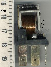
A relay is an electrically operated switch. Current flowing through the coil of the relay creates a magnetic field which attracts a lever and changes the switch contacts. The coil current can be on or off so relays have two switch positions and most have double throw (changeover) switch contacts as shown in the diagram.
Relays allow one circuit to switch a second circuit which can be completely separate from the first. For example a low voltage battery circuit can use a relay to switch a 230V AC mains circuit. There is no electrical connection inside the relay between the two circuits, the link is magnetic and mechanical.
The coil of a relay passes a relatively large current, typically 30mA for a 12V relay, but it can be as much as 100mA for relays designed to operate from lower voltages. Most ICs (chips) cannot provide this current and a transistor is usually used to amplify the small IC current to the larger value required for the relay coil. The maximum output current for the popular 555 timer IC is 200mA so these devices can supply relay coils directly without amplification.


Relays are usuallly SPDT or DPDT but they can have many more sets of switch contacts, for example relays with 4 sets of changeover contacts are readily available. For further information about switch contacts and the terms used to describe them please see the page on switches.
Most relays are designed for PCB mounting but you can solder wires directly to the pins providing you take care to avoid melting the plastic case of the relay.
The supplier's catalogue should show you the relay's connections. The coil will be obvious and it may be connected either way round. Relay coils produce brief high voltage 'spikes' when they are switched off and this can destroy transistors and ICs in the circuit. To prevent damage you must connect a protection diode across the relay coil.


The animated picture shows a working relay with its coil and switch contacts. You can see a lever on the left being attracted by magnetism when the coil is switched on. This lever moves the switch contacts. There is one set of contacts (SPDT) in the foreground and another behind them, making the relay DPDT.

Leds

A light-emitting diode (LED, play /ˌɛl ˈd/ el-ee-dee)[1] is a semiconductor light source. LEDs are used as indicator lamps in many devices and are increasingly used for other lighting. Introduced as a practical electronic component in 1962,[2] early LEDs emitted low-intensity red light, but modern versions are available across the visible, ultraviolet and infrared wavelengths, with very high brightness.

Light Emitting Diodes (LEDs)

Colours | Sizes and shapes | Resistor value | LEDs in series | LED data | Flashing | Displays

Example:   LED    Circuit symbol:   LED circuit symbol

Function

LEDs emit light when an electric current passes through them.


Connecting and soldering

LED connections LEDs must be connected the correct way round, the diagram may be labelled a or + for anode and k or - for cathode (yes, it really is k, not c, for cathode!). The cathode is the short lead and there may be a slight flat on the body of round LEDs. If you can see inside the LED the cathode is the larger electrode (but this is not an official identification method). LEDs can be damaged by heat when soldering, but the risk is small unless you are very slow. No special precautions are needed for soldering most LEDs.

Testing an LED

Testing an LED

Never connect an LED directly to a battery or power supply!
It will be destroyed almost instantly because too much current will pass through and burn it out. LEDs must have a resistor in series to limit the current to a safe value, for quick testing purposes a 1kohm resistor is suitable for most LEDs if your supply voltage is 12V or less. Remember to connect the LED the correct way round!
For an accurate value please see Calculating an LED resistor value below.


Colours of LEDs

LED colours LEDs are available in red, orange, amber, yellow, green, blue and white. Blue and white LEDs are much more expensive than the other colours. The colour of an LED is determined by the semiconductor material, not by the colouring of the 'package' (the plastic body). LEDs of all colours are available in uncoloured packages which may be diffused (milky) or clear (often described as 'water clear'). The coloured packages are also available as diffused (the standard type) or transparent.

Rectifiers

A rectifier is an electrical device that converts alternating current (AC), which periodically reverses direction, to direct current (DC), which is in only one direction, a process known as rectification. Rectifiers have many uses including as components of power supplies and as detectors of radio signals. Rectifiers may be made of solid state diodes, silicon-controlled rectifiers, vacuum tube diodes, mercury arc valves, and other components.
A device which performs the opposite function (converting DC to AC) is known as an inverter...

Now we come to the most popular application of the diode: rectification. Simply defined, rectification is the conversion of alternating current (AC) to direct current (DC). This involves a device that only allows one-way flow of electrons. As we have seen, this is exactly what a semiconductor diode does. The simplest kind of rectifier circuit is the half-wave rectifier. It only allows one half of an AC waveform to pass through to the load. (Figure below)

Half-wave rectifier circuit.
For most power applications, half-wave rectification is insufficient for the task. The harmonic content of the rectifier's output waveform is very large and consequently difficult to filter. Furthermore, the AC power source only supplies power to the load one half every full cycle, meaning that half of its capacity is unused. Half-wave rectification is, however, a very simple way to reduce power to a resistive load. Some two-position lamp dimmer switches apply full AC power to the lamp filament for “full” brightness and then half-wave rectify it for a lesser light output. (Figure below)

Half-wave rectifier application: Two level lamp dimmer.
In the “Dim” switch position, the incandescent lamp receives approximately one-half the power it would normally receive operating on full-wave AC. Because the half-wave rectified power pulses far more rapidly than the filament has time to heat up and cool down, the lamp does not blink. Instead, its filament merely operates at a lesser temperature than normal, providing less light output. This principle of “pulsing” power rapidly to a slow-responding load device to control the electrical power sent to it is common in the world of industrial electronics. Since the controlling device (the diode, in this case) is either fully conducting or fully nonconducting at any given time, it dissipates little heat energy while controlling load power, making this method of power control very energy-efficient. This circuit is perhaps the crudest possible method of pulsing power to a load, but it suffices as a proof-of-concept application.
If we need to rectify AC power to obtain the full use of both half-cycles of the sine wave, a different rectifier circuit configuration must be used. Such a circuit is called a full-wave rectifier. One kind of full-wave rectifier, called the center-tap design, uses a transformer with a center-tapped secondary winding and two diodes, as in Figure below.

Full-wave rectifier, center-tapped design.
This circuit's operation is easily understood one half-cycle at a time. Consider the first half-cycle, when the source voltage polarity is positive (+) on top and negative (-) on bottom. At this time, only the top diode is conducting; the bottom diode is blocking current, and the load “sees” the first half of the sine wave, positive on top and negative on bottom. Only the top half of the transformer's secondary winding carries current during this half-cycle as in Figure below.

Full-wave center-tap rectifier: Top half of secondary winding conducts during positive half-cycle of input, delivering positive half-cycle to load..
During the next half-cycle, the AC polarity reverses. Now, the other diode and the other half of the transformer's secondary winding carry current while the portions of the circuit formerly carrying current during the last half-cycle sit idle. The load still “sees” half of a sine wave, of the same polarity as before: positive on top and negative on bottom. (Figure below)

Full-wave center-tap rectifier: During negative input half-cycle, bottom half of secondary winding conducts, delivering a positive half-cycle to the load.
One disadvantage of this full-wave rectifier design is the necessity of a transformer with a center-tapped secondary winding. If the circuit in question is one of high power, the size and expense of a suitable transformer is significant. Consequently, the center-tap rectifier design is only seen in low-power applications.
The full-wave center-tapped rectifier polarity at the load may be reversed by changing the direction of the diodes. Furthermore, the reversed diodes can be paralleled with an existing positive-output rectifier. The result is dual-polarity full-wave center-tapped rectifier in Figure below. Note that the connectivity of the diodes themselves is the same configuration as a bridge.

Dual polarity full-wave center tap rectifier
Another, more popular full-wave rectifier design exists, and it is built around a four-diode bridge configuration. For obvious reasons, this design is called a full-wave bridge. (Figure below)


Full-wave bridge rectifier.
Current directions for the full-wave bridge rectifier circuit are as shown in Figure below for positive half-cycle and Figure below for negative half-cycles of the AC source waveform. Note that regardless of the polarity of the input, the current flows in the same direction through the load. That is, the negative half-cycle of source is a positive half-cycle at the load. The current flow is through two diodes in series for both polarities. Thus, two diode drops of the source voltage are lost (0.7·2=1.4 V for Si) in the diodes. This is a disadvantage compared with a full-wave center-tap design. This disadvantage is only a problem in very low voltage power supplies.
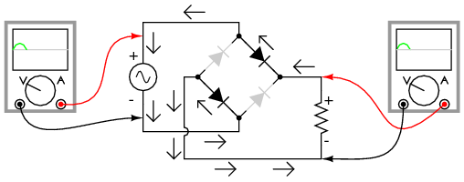
Full-wave bridge rectifier: Electron flow for positive half-cycles.

Full-wave bridge rectifier: Electron flow for negative half=cycles.
Remembering the proper layout of diodes in a full-wave bridge rectifier circuit can often be frustrating to the new student of electronics. I've found that an alternative representation of this circuit is easier both to remember and to comprehend. It's the exact same circuit, except all diodes are drawn in a horizontal attitude, all “pointing” the same direction. (Figure below}

Alternative layout style for Full-wave bridge rectifier.
One advantage of remembering this layout for a bridge rectifier circuit is that it expands easily into a polyphase version in Figure below.
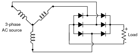
Three-phase full-wave bridge rectifier circuit.
Each three-phase line connects between a pair of diodes: one to route power to the positive (+) side of the load, and the other to route power to the negative (-) side of the load. Polyphase systems with more than three phases are easily accommodated into a bridge rectifier scheme. Take for instance the six-phase bridge rectifier circuit in Figure below.

Six-phase full-wave bridge rectifier circuit.
When polyphase AC is rectified, the phase-shifted pulses overlap each other to produce a DC output that is much “smoother” (has less AC content) than that produced by the rectification of single-phase AC. This is a decided advantage in high-power rectifier circuits, where the sheer physical size of filtering components would be prohibitive but low-noise DC power must be obtained. The diagram in Figure below shows the full-wave rectification of three-phase AC.

Three-phase AC and 3-phase full-wave rectifier output.
In any case of rectification -- single-phase or polyphase -- the amount of AC voltage mixed with the rectifier's DC output is called ripple voltage. In most cases, since “pure” DC is the desired goal, ripple voltage is undesirable. If the power levels are not too great, filtering networks may be employed to reduce the amount of ripple in the output voltage.
Sometimes, the method of rectification is referred to by counting the number of DC “pulses” output for every 360o of electrical “rotation.” A single-phase, half-wave rectifier circuit, then, would be called a 1-pulse rectifier, because it produces a single pulse during the time of one complete cycle (360o) of the AC waveform. A single-phase, full-wave rectifier (regardless of design, center-tap or bridge) would be called a 2-pulse rectifier, because it outputs two pulses of DC during one AC cycle's worth of time. A three-phase full-wave rectifier would be called a 6-pulse unit.
Modern electrical engineering convention further describes the function of a rectifier circuit by using a three-field notation of phases, ways, and number of pulses. A single-phase, half-wave rectifier circuit is given the somewhat cryptic designation of 1Ph1W1P (1 phase, 1 way, 1 pulse), meaning that the AC supply voltage is single-phase, that current on each phase of the AC supply lines moves in only one direction (way), and that there is a single pulse of DC produced for every 360o of electrical rotation. A single-phase, full-wave, center-tap rectifier circuit would be designated as 1Ph1W2P in this notational system: 1 phase, 1 way or direction of current in each winding half, and 2 pulses or output voltage per cycle. A single-phase, full-wave, bridge rectifier would be designated as 1Ph2W2P: the same as for the center-tap design, except current can go both ways through the AC lines instead of just one way. The three-phase bridge rectifier circuit shown earlier would be called a 3Ph2W6P rectifier.
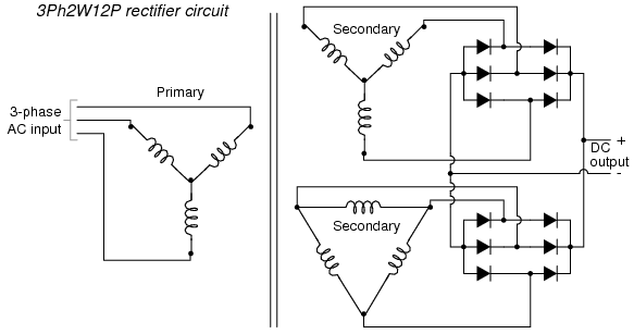
Is it possible to obtain more pulses than twice the number of phases in a rectifier circuit? The answer to this question is yes: especially in polyphase circuits. Through the creative use of transformers, sets of full-wave rectifiers may be paralleled in such a way that more than six pulses of DC are produced for three phases of AC. A 30o phase shift is introduced from primary to secondary of a three-phase transformer when the winding configurations are not of the same type. In other words, a transformer connected either Y-Δ or Δ-Y will exhibit this 30o phase shift, while a transformer connected Y-Y or Δ-Δ will not. This phenomenon may be exploited by having one transformer connected Y-Y feed a bridge rectifier, and have another transformer connected Y-Δ feed a second bridge rectifier, then parallel the DC outputs of both rectifiers. (Figure below Since the ripple voltage waveforms of the two rectifiers' outputs are phase-shifted 30o from one another, their superposition results in less ripple than either rectifier output considered separately: 12 pulses per 360o instead of just six:

Polyphase rectifier circuit: 3-phase 2-way 12-pulse (3Ph2W12P)
  • REVIEW:
  • Rectification is the conversion of alternating current (AC) to direct current (DC).
  • A half-wave rectifier is a circuit that allows only one half-cycle of the AC voltage waveform to be applied to the load, resulting in one non-alternating polarity across it. The resulting DC delivered to the load “pulsates” significantly.
  • A full-wave rectifier is a circuit that converts both half-cycles of the AC voltage waveform to an unbroken series of voltage pulses of the same polarity. The resulting DC delivered to the load doesn't “pulsate” as much.
  • Polyphase alternating current, when rectified, gives a much “smoother” DC waveform (less ripple voltage) than rectified single-phase AC.

Images of filters


Filters

Group Delay Distortion
Depiction of a Group of waves passing through a Typical BandPass Filter

Depiction of a "Group" of waves passing through a Typical BandPass Filter
In an ideal filter all of the waves would pass through with no skew.


LowPass Filter
HighPass Filter Plot   Simple depiction of 
  Filter Characteristics
HighPass Filter

BandPass FIlter

BandReject FIlter, A.K.A., Notch Filter