The Intel 8051 microcontroller is one of the most popular general purpose microcontrollers in use today. The success of the Intel 8051 spawned a number of clones which are collectively referred to as the MCS-51 family of microcontrollers, which includes chips from vendors such as Atmel, Philips, Infineon, and Texas Instruments.
The Intel 8051 is an 8-bit microcontroller which means that most available operations are limited to 8 bits. There are 3 basic "sizes" of the 8051: Short, Standard, and Extended. The Short and Standard chips are often available in DIP (dual in-line package) form, but the Extended 8051 models often have a different form factor, and are not "drop-in compatible". All these things are called 8051 because they can all be programmed using 8051 assembly language, and they all share certain features (although the different models all have their own special features).[edit]About the 8051
Some of the features that have made the 8051 popular are:
- 64 KB on chip program memory.
- 128 bytes on chip data memory(RAM).
- 4 reg banks.
- 128 user defined software flags.
- 8-bit data bus
- 16-bit address bus
- 32 general purpose registers each of 8 bits
- 16 bit timers (usually 2, but may have more, or less).
- 3 internal and 2 external interrupts.
- Bit as well as byte addressable RAM area of 16 bytes.
- Four 8-bit ports, (short models have two 8-bit ports).
- 16-bit program counter and data pointer.
- 1 Microsecond instruction cycle with 12 MHz Crystal.
8051 models may also have a number of special, model-specific features, such as UARTs, ADC, OpAmps, etc...
Typical applications
8051 chips are used in a wide variety of control systems, telecom applications, robotics as well as in the automotive industry. By some estimations, 8051 family chips make up over 50% of the embedded chip market.
]Basic Pin
PIN 9: PIN 9 is the reset pin which is used reset the microcontroller’s internal registers and ports upon starting up. (Pin should be held high for 2 machine cycles.)
PINS 18 & 19: The 8051 has a built-in oscillator amplifier hence we need to only connect a crystal at these pins to provide clock pulses to the circuit.
PIN 40 and 20: Pins 40 and 20 are VCC and ground respectively. The 8051 chip needs +5V 500mA to function properly, although there are lower powered versions like the Atmel 2051 which is a scaled down version of the 8051 which runs on +3V.
PINS 29, 30 & 31: As described in the features of the 8051, this chip contains a built-in flash memory. In order to program this we need to supply a voltage of +12V at pin 31. If external memory is connected then PIN 31, also called EA/VPP, should be connected to ground to indicate the presence of external memory. PIN 30 is called ALE (address latch enable), which is used when multiple memory chips are connected to the controller and only one of them needs to be selected.We will deal with this in depth in the later chapters. PIN 29 is called PSEN. This is "program store enable". In order to use the external memory it is required to provide the low voltage (0) on both PSEN and EA pins.
]Ports
There are 4 8-bit ports: P0, P1, P2 and P3.
PORT P1 (Pins 1 to 8): The port P1 is a general purpose input/output port which can be used for a variety of interfacing tasks. The other ports P0, P2 and P3 have dual roles or additional functions associated with them based upon the context of their usage.
PORT P3 (Pins 10 to 17): PORT P3 acts as a normal IO port, but Port P3 has additional functions such as, serial transmit and receive pins, 2 external interrupt pins, 2 external counter inputs, read and write pins for memory access.
PORT P2 (pins 21 to 28): PORT P2 can also be used as a general purpose 8 bit port when no external memory is present, but if external memory access is required then PORT P2 will act as an address bus in conjunction with PORT P0 to access external memory. PORT P2 acts as A8-A15, as can be seen from fig 1.1
PORT P0 (pins 32 to 39) PORT P0 can be used as a general purpose 8 bit port when no external memory is present, but if external memory access is required then PORT P0 acts as a multiplexed address and data bus that can be used to access external memory in conjunction with PORT P2. P0 acts as AD0-AD7, as can be seen from fig 1.1
[edit]Oscillator Circuits
The 8051 requires the existence of an external oscillator circuit. The oscillator circuit usually runs around 12MHz, although the 8051 (depending on which specific model) is capable of running at a maximum of 40MHz. Each machine cycle in the 8051 is 12 clock cycles, giving an effective cycle rate at 1MHz (for a 12MHz clock) to 3.33MHz (for the maximum 40MHz clock).
]Internal Architecture
]Data and Program Memory
The 8051 Microprocessor can be programmed in PL/M, 8051 Assembly, C and a number of other high-level languages. Many compilers even have support for compiling C++ for an 8051.
Program memory in the 8051 is read-only, while the data memory is considered to be read/write accessible. When stored on EEPROM or Flash, the program memory can be rewritten when the microcontroller is in the special programmer circuit.
]Program Start Address
The 8051 starts executing program instructions from address 0000 in the program memory.
Direct Memory
The 8051 has 256 bytes of internal addressable RAM, although only the first 128 bytes are available for general use by the programmer. The first 128 bytes of RAM (from 0x00 to 0x7F) are called the Direct Memory, and can be used to store data.
]Special Function Register
The Special Function Register (SFR) is the upper area of addressable memory, from address 0x80 to 0xFF. A, B, PSW, DPTR are called SFR.This area of memory cannot be used for data or program storage, but is instead a series of memory-mapped ports and registers. All port input and output can therefore be performed by memory mov operations on specified addresses in the SFR. Also, different status registers are mapped into the SFR, for use in checking the status of the 8051, and changing some operational parameters of the 8051.
]General Purpose Registers
The 8051 has 4 selectable banks of 8 addressable 8-bit registers, R0 to R7. This means that there are essentially 32 available general purpose registers, although only 8 (one bank) can be directly accessed at a time. To access the other banks, we need to change the current bank number in the flag status register.
t]A and B Registers
The A register is located in the SFR memory location 0xE0. The A register works in a similar fashion to the AX register of x86 processors. The A register is called the accumulator, and by default it receives the result of all arithmetic operations. The B register is used in a similar manner, except that it can receive the extended answers from the multiply and divide operations. When not being used for multiplication and Division, the B register is available as an extra general-purpose register.
What is 8051 Standard?
Microcontroller manufacturers have been competing for a long time for attracting choosy customers and every couple of days a new chip with a higher operating frequency, more memory and upgraded A/D converters appeared on the market.
However, most of them had the same or at least very similar architecture known in the world of microcontrollers as “8051 compatible”. What is all this about?
The whole story has its beginnings in the far 80s when Intel launched the first series of microcontrollers called the MCS 051. Even though these microcontrollers had quite modest features in comparison to the new ones, they conquered the world very soon and became a standard for what nowadays is called the microcontroller.
The main reason for their great success and popularity is a skillfully chosen configuration which satisfies different needs of a large number of users allowing at the same time constant expansions (refers to the new types of microcontrollers). Besides, the software has been developed in great extend in the meantime, and it simply was not profitable to change anything in the microcontroller’s basic core. This is the reason for having a great number of various microcontrollers which basically are solely upgraded versions of the 8051 family. What makes this microcontroller so special and universal so that almost all manufacturers all over the world manufacture it today under different name?
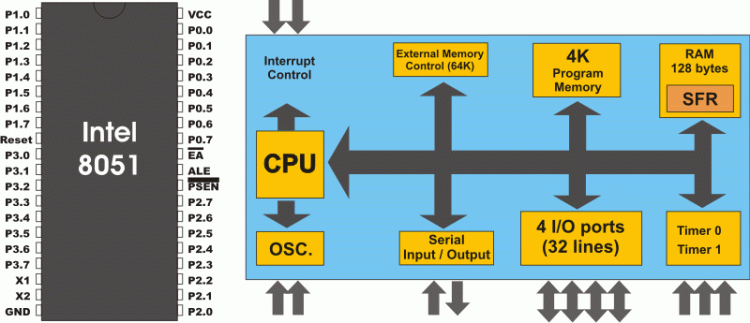
As seen in figure above, the 8051 microcontroller has nothing impressive in appearance:
- 4 Kb of ROM is not much at all.
- 128b of RAM (including SFRs) satisfies the user's basic needs.
- 4 ports having in total of 32 input/output lines are in most cases sufficient to make all necessary connections to peripheral environment.
The whole configuration is obviously thought of as to satisfy the needs of most programmers working on development of automation devices. One of its advantages is that nothing is missing and nothing is too much. In other words, it is created exactly in accordance to the average user‘s taste and needs. Another advantages are RAM organization, the operation of Central Processor Unit (CPU) and ports which completely use all recourses and enable further upgrade.
2.2 Pinout Description
Pins 1-8: Port 1 Each of these pins can be configured as an input or an output.
Pin 9: RS A logic one on this pin disables the microcontroller and clears the contents of most registers. In other words, the positive voltage on this pin resets the microcontroller. By applying logic zero to this pin, the program starts execution from the beginning.
Pins10-17: Port 3 Similar to port 1, each of these pins can serve as general input or output. Besides, all of them have alternative functions:
Pin 10: RXD Serial asynchronous communication input or Serial synchronous communication output.
Pin 11: TXD Serial asynchronous communication output or Serial synchronous communication clock output.
Pin 12: INT0 Interrupt 0 input.
Pin 13: INT1 Interrupt 1 input.
Pin 14: T0 Counter 0 clock input.
Pin 15: T1 Counter 1 clock input.
Pin 16: WR Write to external (additional) RAM.
Pin 17: RD Read from external RAM.
Pin 18, 19: X2, X1 Internal oscillator input and output. A quartz crystal which specifies operating frequency is usually connected to these pins. Instead of it, miniature ceramics resonators can also be used for frequency stability. Later versions of microcontrollers operate at a frequency of 0 Hz up to over 50 Hz.
Pin 20: GND Ground.
Pin 21-28: Port 2 If there is no intention to use external memory then these port pins are configured as general inputs/outputs. In case external memory is used, the higher address byte, i.e. addresses A8-A15 will appear on this port. Even though memory with capacity of 64Kb is not used, which means that not all eight port bits are used for its addressing, the rest of them are not available as inputs/outputs.
Pin 29: PSEN If external ROM is used for storing program then a logic zero (0) appears on it every time the microcontroller reads a byte from memory.
Pin 30: ALE Prior to reading from external memory, the microcontroller puts the lower address byte (A0-A7) on P0 and activates the ALE output. After receiving signal from the ALE pin, the external register (usually 74HCT373 or 74HCT375 add-on chip) memorizes the state of P0 and uses it as a memory chip address. Immediately after that, the ALU pin is returned its previous logic state and P0 is now used as a Data Bus. As seen, port data multiplexing is performed by means of only one additional (and cheap) integrated circuit. In other words, this port is used for both data and address transmission.
Pin 31: EA By applying logic zero to this pin, P2 and P3 are used for data and address transmission with no regard to whether there is internal memory or not. It means that even there is a program written to the microcontroller, it will not be executed. Instead, the program written to external ROM will be executed. By applying logic one to the EA pin, the microcontroller will use both memories, first internal then external (if exists).
Pin 32-39: Port 0 Similar to P2, if external memory is not used, these pins can be used as general inputs/outputs. Otherwise, P0 is configured as address output (A0-A7) when the ALE pin is driven high (1) or as data output (Data Bus) when the ALE pin is driven low (0).
Pin 40: VCC +5V power supply.
2.3 Input/Output Ports (I/O Ports)
All 8051 microcontrollers have 4 I/O ports each comprising 8 bits which can be configured as inputs or outputs. Accordingly, in total of 32 input/output pins enabling the microcontroller to be connected to peripheral devices are available for use.
Pin configuration, i.e. whether it is to be configured as an input (1) or an output (0), depends on its logic state. In order to configure a microcontroller pin as an input, it is necessary to apply a logic zero (0) to appropriate I/O port bit. In this case, voltage level on appropriate pin will be 0.
Similarly, in order to configure a microcontroller pin as an input, it is necessary to apply a logic one (1) to appropriate port. In this case, voltage level on appropriate pin will be 5V (as is the case with any TTL input). This may seem confusing but don't loose your patience. It all becomes clear after studying simple electronic circuits connected to an I/O pin.
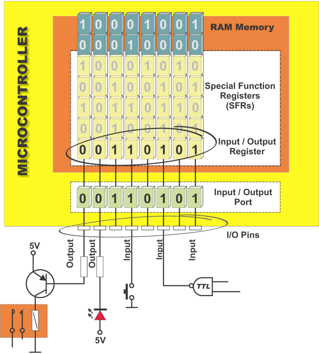
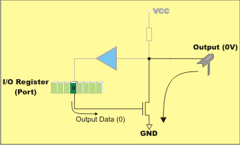
Input/Output (I/O) pin
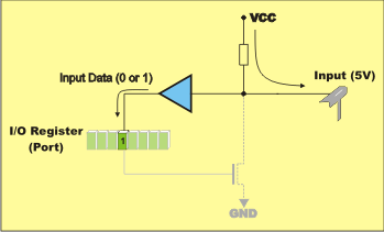
Figure above illustrates a simplified schematic of all circuits within the microcontroler connected to one of its pins. It refers to all the pins except those of the P0 port which do not have pull-up resistors built-in.
Figure above illustrates a simplified schematic of all circuits within the microcontroler connected to one of its pins. It refers to all the pins except those of the P0 port which do not have pull-up resistors built-in.
Output pin
A logic zero (0) is applied to a bit of the P register. The output FE transistor is turned on, thus connecting the appropriate pin to ground.
A logic zero (0) is applied to a bit of the P register. The output FE transistor is turned on, thus connecting the appropriate pin to ground.
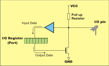
Input pin
A logic one (1) is applied to a bit of the P register. The output FE transistor is turned off and the appropriate pin remains connected to the power supply voltage over a pull-up resistor of high resistance.
A logic one (1) is applied to a bit of the P register. The output FE transistor is turned off and the appropriate pin remains connected to the power supply voltage over a pull-up resistor of high resistance.

Logic state (voltage) of any pin can be changed or read at any moment. A logic zero (0) and logic one (1) are not equal. A logic one (0) represents a short circuit to ground. Such a pin acts as an output.
A logic one (1) is “loosely” connected to the power supply voltage over a resistor of high resistance. Since this voltage can be easily “reduced” by an external signal, such a pin acts as an input.
Port 0
The P0 port is characterized by two functions. If external memory is used then the lower address byte (addresses A0-A7) is applied on it. Otherwise, all bits of this port are configured as inputs/outputs.
The other function is expressed when it is configured as an output. Unlike other ports consisting of pins with built-in pull-up resistor connected by its end to 5 V power supply, pins of this port have this resistor left out. This apparently small difference has its consequences:
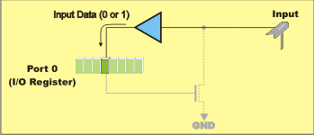
If any pin of this port is configured as an input then it acts as if it “floats”. Such an input has unlimited input resistance and indetermined potential.
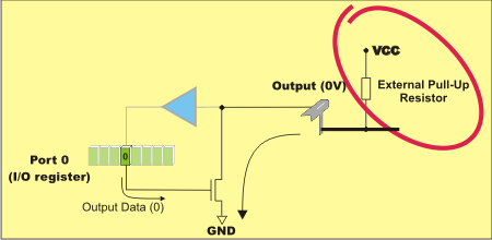
When the pin is configured as an output, it acts as an “open drain”. By applying logic 0 to a port bit, the appropriate pin will be connected to ground (0V). By applying logic 1, the external output will keep on “floating”. In order to apply logic 1 (5V) on this output pin, it is necessary to built in an external pull-up resistor.

Only in case P0 is used for addressing external memory, the microcontroller will provide internal power supply source in order to supply its pins with logic one. There is no need to add external pull-up resistors.
Port 1
P1 is a true I/O port, because it doesn't have any alternative functions as is the case with P0, but can be cofigured as general I/O only. It has a pull-up resistor built-in and is completely compatible with TTL circuits.
Port 2
P2 acts similarly to P0 when external memory is used. Pins of this port occupy addresses intended for external memory chip. This time it is about the higher address byte with addresses A8-A15. When no memory is added, this port can be used as a general input/output port showing features similar to P1.
Port 3
All port pins can be used as general I/O, but they also have an alternative function. In order to use these alternative functions, a logic one (1) must be applied to appropriate bit of the P3 register. In tems of hardware, this port is similar to P0, with the difference that its pins have a pull-up resistor built-in.
Pin's Current limitations
When configured as outputs (logic zero (0)), single port pins can receive a current of 10mA. If all 8 bits of a port are active, a total current must be limited to 15mA (port P0: 26mA). If all ports (32 bits) are active, total maximum current must be limited to 71mA. When these pins are configured as inputs (logic 1), built-in pull-up resistors provide very weak current, but strong enough to activate up to 4 TTL inputs of LS series.

As seen from description of some ports, even though all of them have more or less similar architecture, it is necessary to pay attention to which of them is to be used for what and how.
For example, if they shall be used as outputs with high voltage level (5V), then P0 should be avoided because its pins do not have pull-up resistors, thus giving low logic level only. When using other ports, one should have in mind that pull-up resistors have a relatively high resistance, so that their pins can give a current of several hundreds microamperes only.
2.4 Memory Organization
The 8051 has two types of memory and these are Program Memory and Data Memory. Program Memory (ROM) is used to permanently save the program being executed, while Data Memory (RAM) is used for temporarily storing data and intermediate results created and used during the operation of the microcontroller. Depending on the model in use (we are still talking about the 8051 microcontroller family in general) at most a few Kb of ROM and 128 or 256 bytes of RAM is used. However…
All 8051 microcontrollers have a 16-bit addressing bus and are capable of addressing 64 kb memory. It is neither a mistake nor a big ambition of engineers who were working on basic core development. It is a matter of smart memory organization which makes these microcontrollers a real “programmers’ goody“.
Program Memory
The first models of the 8051 microcontroller family did not have internal program memory. It was added as an external separate chip. These models are recognizable by their label beginning with 803 (for example 8031 or 8032). All later models have a few Kbyte ROM embedded. Even though such an amount of memory is sufficient for writing most of the programs, there are situations when it is necessary to use additional memory as well. A typical example are so called lookup tables. They are used in cases when equations describing some processes are too complicated or when there is no time for solving them. In such cases all necessary estimates and approximates are executed in advance and the final results are put in the tables (similar to logarithmic tables).
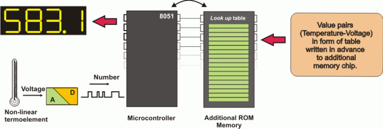
How does the microcontroller handle external memory depends on the EA pin logic state:
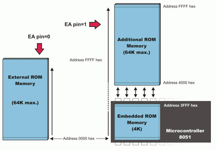
EA=0 In this case, the microcontroller completely ignores internal program memory and executes only the program stored in external memory.
EA=1 In this case, the microcontroller executes first the program from built-in ROM, then the program stored in external memory.
In both cases, P0 and P2 are not available for use since being used for data and address transmission. Besides, the ALE and PSEN pins are also used.
Data Memory
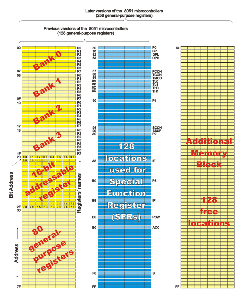
As already mentioned, Data Memory is used for temporarily storing data and intermediate results created and used during the operation of the microcontroller. Besides, RAM memory built in the 8051 family includes many registers such as hardware counters and timers, input/output ports, serial data buffers etc. The previous models had 256 RAM locations, while for the later models this number was incremented by additional 128 registers. However, the first 256 memory locations (addresses 0-FFh) are the heart of memory common to all the models belonging to the 8051 family. Locations available to the user occupy memory space with addresses 0-7Fh, i.e. first 128 registers. This part of RAM is divided in several blocks.
The first block consists of 4 banks each including 8 registers denoted by R0-R7. Prior to accessing any of these registers, it is necessary to select the bank containing it. The next memory block (address 20h-2Fh) is bit- addressable, which means that each bit has its own address (0-7Fh). Since there are 16 such registers, this block contains in total of 128 bits with separate addresses (address of bit 0 of the 20h byte is 0, while address of bit 7 of the 2Fh byte is 7Fh). The third group of registers occupy addresses 2Fh-7Fh, i.e. 80 locations, and does not have any special functions or features.
Additional RAM
In order to satisfy the programmers’ constant hunger for Data Memory, the manufacturers decided to embed an additional memory block of 128 locations into the latest versions of the 8051 microcontrollers. However, it’s not as simple as it seems to be… The problem is that electronics performing addressing has 1 byte (8 bits) on disposal and is capable of reaching only the first 256 locations, therefore. In order to keep already existing 8-bit architecture and compatibility with other existing models a small trick was done.
What does it mean? It means that additional memory block shares the same addresses with locations intended for the SFRs (80h- FFh). In order to differentiate between these two physically separated memory spaces, different ways of addressing are used. The SFRs memory locations are accessed by direct addressing, while additional RAM memory locations are accessed by indirect addressing.
Memory expansion
In case memory (RAM or ROM) built in the microcontroller is not sufficient, it is possible to add two external memory chips with capacity of 64Kb each. P2 and P3 I/O ports are used for their addressing and data transmission.
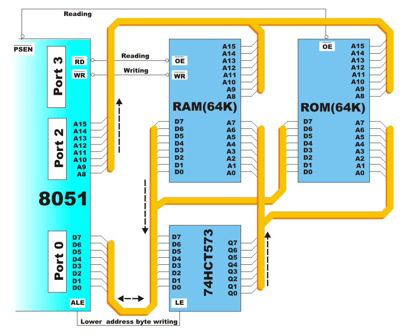
From the user’s point of view, everything works quite simply when properly connected because most operations are performed by the microcontroller itself. The 8051 microcontroller has two pins for data read RD#(P3.7) and PSEN#. The first one is used for reading data from external data memory (RAM), while the other is used for reading data from external program memory (ROM). Both pins are active low. A typical example of memory expansion by adding RAM and ROM chips (Hardward architecture), is shown in figure above.
Even though additional memory is rarely used with the latest versions of the microcontrollers, we will describe in short what happens when memory chips are connected according to the previous schematic. The whole process described below is performed automatically.
- When the program during execution encounters an instruction which resides in external memory (ROM), the microcontroller will activate its control output ALE and set the first 8 bits of address (A0-A7) on P0. IC circuit 74HCT573 passes the first 8 bits to memory address pins.
- A signal on the ALE pin latches the IC circuit 74HCT573 and immediately afterwards 8 higher bits of address (A8-A15) appear on the port. In this way, a desired location of additional program memory is addressed. It is left over to read its content.
- Port P0 pins are configured as inputs, the PSEN pin is activated and the microcontroller reads from memory chip.
Similar occurs when it is necessary to read location from external RAM. Addressing is performed in the same way, while read and write are performed via signals appearing on the control outputs RD (is short for read) or WR (is short for write).
Addressing
While operating, the processor processes data as per program instructions. Each instruction consists of two parts. One part describes WHAT should be done, while the other explains HOW to do it. The latter part can be a data (binary number) or the address at which the data is stored. Two ways of addressing are used for all 8051 microcontrollers depending on which part of memory should be accessed:
Direct Addressing
On direct addressing, the address of memory location containing data to be read is specified in instruction. The address may contain a number being changed during operation (variable). For example:
Since the address is only one byte in size (the largest number is 255), only the first 255 locations of RAM can be accessed this way. The first half of RAM is available for use, while another half is reserved for SFRs.
MOV A,33h; Means: move a number from address 33 hex. to accumulator
Indirect Addressing
On indirect addressing, a register containing the address of another register is specified in instruction. Data to be used in the program is stored in the letter register. For example:
Indirect addressing is only used for accessing RAM locations available for use (never for accessing SFRs). This is the only way of accessing all the latest versions of the microcontrollers with additional memory block (128 locations of RAM). Simply put, when the program encounters instruction including “@” sign and if the specified address is higher than 128 ( 7F hex.), the processor knows that indirect addressing is used and skips memory space reserved for SFRs.
MOV A,@R0; Means: Store the value from the register whose address is in the R0 register
into accumulator
On indirect addressing, registers R0, R1 or Stack Pointer are used for specifying 8-bit addresses. Since only 8 bits are avilable, it is possible to access only registers of internal RAM this way (128 locations when speaking of previous models or 256 locations when speaking of latest models of microcontrollers). If an extra memory chip is added then the 16-bit DPTR Register (consisting of the registers DPTRL and DPTRH) is used for specifying address. In this way it is possible to access any location in the range of 64K


No comments:
Post a Comment